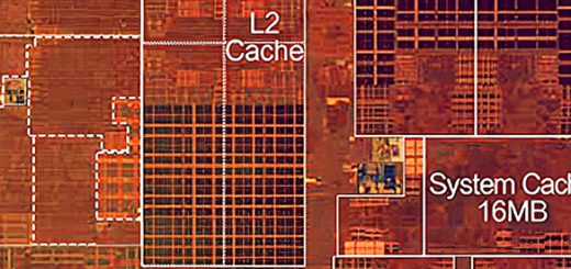
APPLE M1 DIESHOT

Image from techinsights/APPLE official website.
Floor Plan by me.
| M1 | area(mm^2) | size(MiB) | SRAM density(MB/mm^2) |
| Firestorm L2 | 3.500539165 | 12 | 3.428043348 |
| Icestorm L2 | 1.228958081 | 4 | 3.254789614 |
| SLC | 2.45910606 | 8 | 3.253214707 |
| TSMC 5nm HP | 3.688064141 | 12 | 3.253739507 |
| TSMC 5nm HD | 3.500539165 | 12 | 3.428043348 |
| total | 7.188603306 | 24 | 3.338617945 |
| M1(TSMC 5nm HD) | M1(TSMC 5nm HP) | A14(TSMC 5nm HD) | A14(TSMC 5nm HP) | Lakefield(Intel 10nmSF) | SD855(TSMC 7nm DUV HD) | K980(TSMC 7nm DUV HD) | KX5000(HLMC 28nm) | |
| SRAM density | 3.428043348 | 3.253739507 | 3.669986689 | 3.35286302 | 1.675987565 | 2.463892974 | 2.386652552 | 0.407069712 |
| Relative upshift | 0.00% | 5.36% | -6.59% | 2.24% | 104.54% | 39.13% | 43.63% | 742.13% |
APLLE M1 die size is at about 120.5mm^2.
TSMC 5nm can be reach for a great improvement in density side(about 35-40% to TSMC 7nm,and in some case it looks even better.TSMC 7nm also in some case keep at about 1.6MB/mm^2,in that case,5nm can reach out 100% provement in density).
Of course, for more logic circure or I/O,it can be lower improvement at density side for more improving perfromance.
Cuz there are not any accuracte data of M1/A14’s Diesize,so data are not totally accuracte.


GPU core怎么只有7个?